![[The TNT Convertus]](../gif/convertus.gif)
First of all we must clearly state the requirements of this design.
Now that I explained all this things, I could tell you that the chip set chosen for this Dac has been selected after long listening tests, exclusively looking for sonic performance and disregarding any other less than noble parameter.
Instead what happened is fairly simpler....
A major problem for DIY people, at least here in Italy, is to find someone available to sell you this kind of components. It is quite clear that if you go on asking friends you can end up with any component you need, but if you want to propose a design for DIY you must find a freely accessible sales channel.
Well, I must say that I have not really found a channel accessible to anyone, but at least I have found a channel my supplier is available to access for me, so that I have only to spend some more money to can get whatever I like. References later.
Given the scarce availability of these products, often what you can find is rather not up to date.
One fundamental point was even the availability of a DIL package: in facts I note that most recent design tend to be available only in surface mount (SMD) packages, which cannot be handled by normal DIY people, even though their manual handling and mounting is not completely impossible...
This could sometimes be solved using special sockets, but it seems that sockets for some packages are not available at all. If you know what I am talking about, you can well understand the problem: you simply should iron solder pins that can be about 0.3mm wide and 0.65mm apart!!!
Just to get to the point, I had to select one of the few chip sets I was able to find, taking into account that the design had to be as simple as possible. I was initially rather doubtful on the chip set, which is rather oldish indeed, but I make up my mind taking into account a few points.
First, this is not simply a kit to be proposed as-is. I wanted to use the design just to introduce the less experienced reader into digital and mixed signal design, which not so many audio DIY people seem to like, and especially to show that the design and building of a DAC is definitely not so complex.
I would like to make you able to get all the information you need directly at their source and to learn how to use them.
Second, I wanted would like to discuss a few problems with DACs trying to explain what is really happening in the simplest way; and to discuss this kind of things an especially complex Dac is not required: if it is a didactic design, than the simplest the better.
Third, while I was testing my own DAC based on the chip I had selected, and I was getting rather disappointed as I could not hear any great progress compared for example with my Linn Mimik, Thorsten told me about Kusunoki's DAC and I decided to do test even a solution based on its concept; it is by the way even less expensive than the other one, so... But what I really did not expected (I know I was wrong: any time Thorsten gives you an advice, you can be sure it is an exceptional advice...) was that very soon I feel in love with its sound and decided that it would be the Convertus official circuit.
So the search ended with CS8412 Digital Receiver and the old TDA1543 16bit stereo D/A converters.
The receiver is a good component, it is well known for a rather good rejection to jitter (less than 200ps output jitter). The DAC instead is a very low cost, old component, normally used after an oversampling filter, that here is instead missing.
The CS8412 is a rather versatile chip which allows to receive an S/PDIF flow and extract from this all the digital signals required by a DAC.
The chip is built up of a set of different functional blocks.
First comes an RS422 differential line receiver, to which can be directly connected the S/PDIF interface input terminal (in case of an optical interface an optocoupler is obviously required, while for AES interface a transformer is strongly recommended and for EBU is mandatory).
Digital data extracted by the line receiver is then passed to a clock and data recovery block, which, using an on-chip PLL (phase locked loop) extracts the master clock (MCK) and data from the flow.
Finally the data flow is sent to the so called audio serial port block where the different piece of information are organised in order to be presented to the output pins. The audio output interface can be set up in a variety of standard or non standard configurations by special mode selection pins.
The fundamental signals present in this interface are
The interface can be configured so that SCK and FSYNC are output, derived from the master clock, or input. Even in this last case MCK is available as an output, so that it is possible to use a separate high stability PLL based on a voltage controlled crystal oscillator (VCXO) to derive a very stable clock from the master clock and derive from this an external SCK ed FSYNC, so that the whole audio interface is based on the external super low jitter clock. This is all the action performed by quite a few (even expensive) reclocking units: the interface in facts can be configured to emit the same received biphase data with the new clock.
In our case we are trying to make things as simple as possible, hence we will stick to the internal clocks.
The audio interface is hence programmed in mode 0, but I could have decided to use any other mode compatible with CS4329 DAC chip, for example the mode 2, which is compatible with the I2S interface used by other DACs.
A 1kohm resistor in parallel with a 0.047uF capacitor must be also connected from the FILT pin, which is the PLL filter pin, to analog ground (we'll se later on the power supply arrangements).
Finally, just to be completely safe, we can make use of the fact that the chip make de-emphasis information available on the so called multifunction pins. These are a set of pins which make available either the error and frequency information (pin SEL low) or the channel status information (SEL high); in our case (consumer) leaving SEL high we could get the de-emphasis information on pin Cc, and use it to control de-emphasis on the DAC; as I have no CDs with deemphasis, I just left this circuit out. Original Kusunoki DAC (and also a previous version of mine) instead used it.
In order to have an ultra high quality digital input interface connection, I choose to use a 75ohm BNCinput connector. Note anyway that this solution, even though better, is not compliant with the S/PDIF standard, which requires a RCA pin.
Anyway the Mimik digital output use BNC too, so in this way I could use a normal BNC/BNC wire, with all 75ohm components in the interconnection. I used a standard quality 75 ohm wire (RG59/U), but the input quality level is probably depending on the interface connection quality (the eye pattern looks quite deformed, at the oscilloscope) so I would suggest you to test different wires; personally, I was not able to hear any difference (any bad effect on sound) even making strange and forbidden things with it...
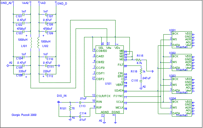
The DAC is even simpler to use. It is really not much more than a simple DAC: there only is the input serial register and control, a DAC and a circuit to keep the output stable between one conversion and the other.
First of all, there obviously is a three wire I2C serial interface: no way of programming it.
Data received from the serial interface is latched in a register and drives directly the 16 bit converter, which hence has a constant current output during each sampling period.
Nothing else.
The I2S connection from the receiver to the DAC is in the end limited to three digital signals. They are
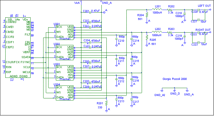
One non minor detail: in our design the TDA1543 is used in a 4X parallel configuration; its output stage voltage swing seems not to be so much limited, but to get a 2 Vrms output it is necessary to drive it with a rather high supply voltage (8.8V), very near its absolute maximum ratings (9V).
An accurate regulation is therefore required: it is necessary to power it up without the DAC chips (or disconnecting the power supply from the DAC chips), which by the way drive a lot of current (60mA and more) ad set the supply voltage to less than 8V, power it off, inserting the DAC chips, power it on again, switch the CD transport on checking that some sound vaguely correct is coming out of the analog output, and set the supply voltage to the target value. If possible you should better also check that distortion at 1 KHz is very low.
Initially, in the first version, I followed the instructions setting up an OP-AMP low-pass output stage. This was largely unsatisfying: the sound was not so transparent and its musicality was poor. In the end I decided to go for a far simpler solution, and set up the very simple configuration I use up to now.
It was slightly changed when I decided to use TDA1543, as this has a current output. In facts currently the IV conversion is performed by a 680 ohm resistor in parallel with four 680pF film capacitors (one on each converter output as near as possible to this), implementing a 344KHz first order low pass filter; after this there is a very simple second order passive LRC low pass filter, which has scarcely any effect on the whole audio band, including its top end, but cuts rather drastically any frequency higher than a few hundred kHz, followed by a coupling capacitor to tear away the DC component (about 2.2V at the output of the DAC chip).
Hence, the output stage is nearly not existent. To make it utterly transparent, the output capacitor is implemented with a 10uF good quality film capacitor (WIMA) in parallel with a 0.47uF paper in oil Jansen capacitor.
Chip designers create objects whose usage, especially for the most complex ones, has been completely predefined in the subtlest details. To obtain better performances from these objects is very difficult and often expensive: it is often necessary simply to substitute some of the inner blocks, where the interstage signal is made available, with external complex circuitry. In most cases all the designer can do is to play around with the available tokens (chips) and combine them in different ways.
In the case of our chips, and especially for the DAC, there is not so much you can do. The possible action areas are essentially the output stage, but we have stripped it down to the basic, and the power supplies.
In the end I decided to set up the best possible PSU arrangement: there is a completely separated PSU, including the transformer, for each of the three independent power supplies required by the chips.
The first PSU is the receiver digital PSU, named PSU-D; its filtering capacitors are not so high as in the other PSUs, but the structure is always very similar. There is a 30VA toroidal transformer with the two 12V secondaries in parallel, followed by superfast full-wave rectification, a first CLC filter, a voltage regulation unit with zener and a trimmer to set the output voltage precisely to 5V and another capacitor followed by an 1000uF inductor, and finally another CLC filter, placed on the DAC card. Note that inductors throughout this design are not used to reduce 50Hz ripple, but just to avoid high frequency noise present on chips power supply pins to go back and be irradiated by all the PSU circuit.
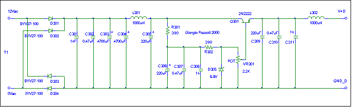
The second PSU, named PSU-A2 is the receiver analogue PSU; it is used to supply a very clean voltage to the PLL circuit, allowing it to work correctly and reducing jitter drastically. The structure is definitely similar to the previous one, always with a second 30VA transformer, but the capacitor values are definitely higher Note that here too there is a CLC filter on the DAC card.
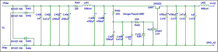
Both these transformers are far more powerful than needed, probably they do not give any benefit with respect to 10VA ones: the reason for this value is just that my usual supplier had no toroidal under 30VA, and anyway price differences are not so high.
The third and last PSU, PSU-A, is the DACs power supply unit. The DACs have only one power supply, that must therefore be treated as an analogue supply voltage. They require a rather high current (I found something like 80mA each, in the end, for a 300mA in total) so the PSU is slightly different.
There is a 50VA or more transformer followed by the rectifier diodes but no first LC filter (you can have one, but you should find a 1mH inductor with a DC resistance less than 1 ohm): the rectifier diodes bridge is directly connected to a first set of four 4700uF capacitors in parallel; then there is a very simple FET voltage regulation unit, with a trimmer to precisely set the supply voltage, another couple of 4700uF capacitors and a 1000uH inductor; on the DAC card there finally is a 0.47uF capacitor near the power supply input pins, and a 4700uF capacitor in parallel with a 0.47uF capacitor for each TDA1543 chip, as near as possible to this. The FET needs a heat sink.
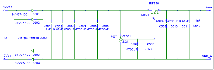
As a total there are about 100,000uF around.
Most filter capacitors are in practice made up of a high value (typically 4700uF) electrolytic capacitor, a good quality film capacitor (typically 0,47uF) and a ceramic capacitor, to be absolutely transparent to high frequencies. The inductors often have also a ferrite pearl in series.
The DAC components are distributed on two boards, one for power supplies and one for digital and analogue circuits.
A good practice is to use ultra fast optocouplers to isolate the analog board from the receiver. In our case I could not use them mainly because I was not able to find any optocoupler fast enough, but I suspect that they could also make jitter a little worse; obviously I have no proof, the measure of jitter is not easy at all, so it is should better be considered a stupid idea. Anyway for a stripped down DAC it is for sure not a major problem.
Just to be sure and keep down the RF garbage amount coming from the receiver I added a set of RF ferrite pearls on each of the leads connecting the receiver to the DAC. Other pearls are inserted on the power supply leads in series with the last RF inductor towards the receiver chips.
The chips are mounted on the copper side of a normal single side printed circuit board; the copper side is used as a set of ground planes: there are three independent (but interconnected in one point) areas, one for each power supply.
The structure of the first two, the receiver digital and analog ground planes, is derived from the layout of the Crystal CS4329-4390 evaluation board; the DAC area has no special requirement, apart the fact that all analogue circuit components and the DAC chips must be mounted on it.
The pin mounting holes through the board have been bevelled with a much larger drill point on the copper side, so that improper contact between pins and ground plane is not possible. On the other side all connections are made using directly the component pins wherever possible, and using single core copper wire in the other cases.
DAC ground pins are not connected to ground plane, but have a separated ground wire which connects to the ground plane in the same place as the ground wire from PSU-D.
I tried to keep the layout of the DAC board as ordered as possible; the digital input comes first, then the receiver, after this the BAC chips, one beside the other with the digital side (all digital input are on one side of the chisp and the analogue outpts on the other) towards the receiver, hence the analogue circuits, the output coupling capacitors and the output pins: all input and outputs are on the same side of the board.
In the cabinet, you should be able to use also a 1-unit 19" rack cabinet, all functional blocks must be orderly placed: first the power supply IEC connector with an RF filter and a fuse, then the power supply transformers, the power supply units board and finally the receiver/DAC board.
Another option, most useful for those that want in time test different DACs, could be to use a separate board for the DAC and connect it to the receiver one through some type of connector. I used this option, as it made testing different chips very simple, but if you care more for sound than for technology, as you should, you should better use a single board for both receiver and DACs.
This is a very unconventional DAC. The measures you get out of it are somewhat surprising and disappointing at the same time.
When you look at the reconstruction of a single sample pulse, first you note that it is as clean and square as possible, without any ringing before or after it, but after a while it appears clear that there is another major problem: the pulse duration is one period long, while it should be as short as possible. So it is quite different, but I am not so sure it is really better than the current DACs one.
The frequency response is almost not measurable at the top end: the signal beats with the sampling frequency, producing what on the oscilloscope seems a modulated tone. This is the naked output of a 44.1Ksps DAC: there is no oversampling and no low pass reconstruction filter. The only slight filtering effect is the sin(x)/x filtering due to the sample and hold mechanism.
The absence of any electronic antialiasing filter causes the aliased lines to be present in quantity; the only filtering effect is again the sin(x)/x.
In the end, only one suggestion: listen to it, before measuring it....
Which music to play with a minimalist DAC? But minimalist music, obviously. So I could suggest you "Music for 18 Musicians" by Steve Reich. (ehm... please before buying it you should better listen to it... it really set new standards in music.... but I would not like to be chased by angry folks trying to hang me up... yes, you would definitely better listen to it: I like contemporary music, but I can imagine other people could be, say, less interested in it...).
The DAC is able to offer a good performance with any kind of music: it perfect is quite good for rock, but also classical and baroque music get a brand new look with it. Its sound is very pequliar, this is the reason I chose this design compared with the more advanced other option I tested (it was CS8412 + CS4329).
Just to try to explain it, i can say that it sounds natural. It is not at all euphonic, it just reports what is on the CD you are playing. There is a complete and still not edgy top end (unless it was recorded edgy), the bass is full, fast.
What, according to me, is missing is - apparently - a little ondulation in frequency responce that any DAC I have listened to has and it is responsible for that not completely natural, a little coloured, abnormally brilliant sound we are used to from most DACs.
Now I should start telling you that this DAC is far better than any other in the world, and that for just a couple of million dollars it is really a great bargain.
Well, I am not completely sure it is really very good. What I can say is that it's sound is, according to me, more similar to the black disc sound than any other DAC's I have listened to and that even other people listening to it noted the difference with the others DACs.
I can also say that I never get tired listening to it. And I can also say that when I go to listen another DAC I constantly come back to listen to this one. Its inconspicuous, low profile, understated sound is really peculiar.
But these are the designer's own words about his creature. Don't believe me, guys. Instead, please note it is really rather inexpensive (I would say 150 US $), you can probably afford it. So you should better build it and then listen to it, and then tell me what you think.
The original Kusunoki information can be found in http://www.geocities.com/ResearchTriangle/8231/
and
http://www.sakurasystems.com/reviews/a2.kusunoki.html.
It's an interesting reading, I really suggest you to go through it.
Copyright 2000 Giorgio Pozzoli - http://www.tnt-audio.com
How to print this article